SystemPlus Consulting publishes a reverse engineering report of Synaptics’ under-display fingerprint scanner found inside the VIVO X21 UD Smartphone:
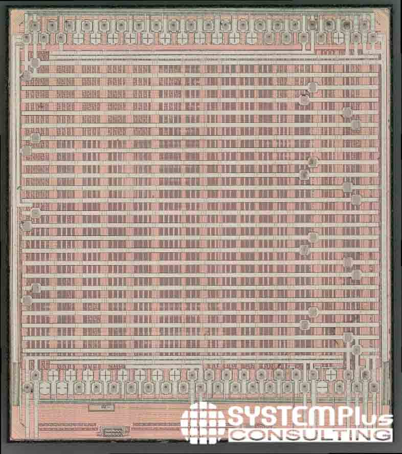
"This scanner uses optical fingerprint technology that allows integration under the display. With a stainless steel support and two flexible printed circuit layers, the Synaptics fingerprint sensor’s dimensions are 6.46 mm x 9.09 mm, with an application specific integrated circuit (ASIC) driver in the flex module. This image sensor is also assembled with a glass substrate where filters are deposited.
The sensor has a resolution of 30,625 pixels, with a pixel density of 777ppi. The module’s light source is providing by the OLED display glasses. The fingerprint module uses a collimator layer corresponding to the layers directly deposited on the die sensor and composed of organic, metallic and silicon layers. This only allows light rays reflected at normal incidence to the collimator filter layer to pass through and reach the optical sensing elements. The sensor is connected by wire bonding to the flexible printed circuit and uses a CMOS process."

 |
| Sensor die |
 |
| ASIC die |
 |
| Optical filter deposition on glass substrate |
Comments
Post a Comment