OSA Optics Express publishes a paper "Dynamic range extension for photon counting arrays" by Ivan Michel Antolovic, Claudio Bruschini, and Edoardo Charbon from TU Delft and EPFL.
"In this paper, we present a thorough analysis, which can actually be applied to any photon counting detector, on how to extend the SPAD dynamic range by exploiting the nonlinear photon response at high count rates and for different recharge mechanisms. We applied passive, active event-driven and clock-driven (i.e. clocked, following quanta image sensor response) recharge directly to the SPADs. The photon response, photon count standard deviation, signal-to-noise ratio and dynamic range were measured and compared to models. Measurements were performed with a CMOS SPAD array targeted for image scanning microscopy, featuring best-in-class 11 V excess bias, 55% peak photon detection probability at 520 nm and >40% from 440 to 640 nm. The array features an extremely low median dark count rate below 0.05 cps/μm2 at 9 V of excess bias and 0°C. We show that active event-driven recharge provides ×75 dynamic range extension and offers novel ways for high dynamic range imaging. When compared to the clock-driven recharge and the quanta image sensor approach, the dynamic range is extended by a factor of ×12.7-26.4. Additionally, for the first time, we evaluate the influence of clock-driven recharge on the SPAD afterpulsing."

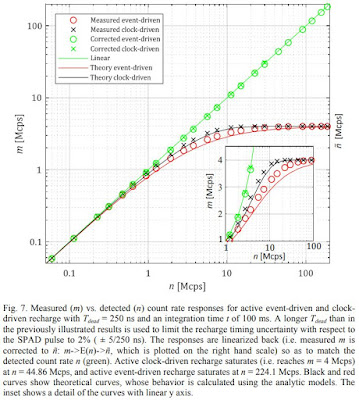
"In this paper, we present a thorough analysis, which can actually be applied to any photon counting detector, on how to extend the SPAD dynamic range by exploiting the nonlinear photon response at high count rates and for different recharge mechanisms. We applied passive, active event-driven and clock-driven (i.e. clocked, following quanta image sensor response) recharge directly to the SPADs. The photon response, photon count standard deviation, signal-to-noise ratio and dynamic range were measured and compared to models. Measurements were performed with a CMOS SPAD array targeted for image scanning microscopy, featuring best-in-class 11 V excess bias, 55% peak photon detection probability at 520 nm and >40% from 440 to 640 nm. The array features an extremely low median dark count rate below 0.05 cps/μm2 at 9 V of excess bias and 0°C. We show that active event-driven recharge provides ×75 dynamic range extension and offers novel ways for high dynamic range imaging. When compared to the clock-driven recharge and the quanta image sensor approach, the dynamic range is extended by a factor of ×12.7-26.4. Additionally, for the first time, we evaluate the influence of clock-driven recharge on the SPAD afterpulsing."


Comments
Post a Comment