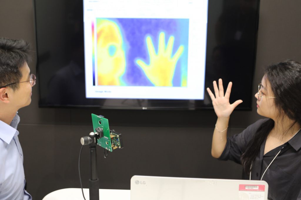
PRNewswire: LG Innotek is entering the thermal imaging infrared camera module business. The company is accelerating the in-house development of core technologies from sensors to module design and production process to develop thermal imaging camera modules.
LG Innotek is confident that it will be able to achieve world-class quality in the design and production of thermal imaging camera modules. This is because the structure and manufacturing process of this module is similar to those of the smartphone camera module. The company has been the number one in the global smartphone camera module market for 7 consecutive years.
Park Jong-seok, CEO of the company, said, "We will continue to release competitive thermal imaging camera modules so that they can be utilized more widely in various areas."
The company believes that improving the performance and lowering the price will expand the market rapidly as the utility value of the thermal camera has already been proven. The first goal is to expand the market from military application to non-military applications such as home appliances, automobiles, and drones. The thermal imaging camera module can be applied to ADAS as well as to autonomous driving system to improve driving safety.
LG Innotek is expanding its cooperation with domestic venture companies to secure thermal imaging sensor technology. Recently, the company started the joint development of the next generation thermal imaging sensor together with Truwin.
According to Yole Developpement, the global thermal imaging camera market is expected to grow from $3,325m in 2018 to $4,385m in 2022.

LG Innotek is confident that it will be able to achieve world-class quality in the design and production of thermal imaging camera modules. This is because the structure and manufacturing process of this module is similar to those of the smartphone camera module. The company has been the number one in the global smartphone camera module market for 7 consecutive years.
Park Jong-seok, CEO of the company, said, "We will continue to release competitive thermal imaging camera modules so that they can be utilized more widely in various areas."
The company believes that improving the performance and lowering the price will expand the market rapidly as the utility value of the thermal camera has already been proven. The first goal is to expand the market from military application to non-military applications such as home appliances, automobiles, and drones. The thermal imaging camera module can be applied to ADAS as well as to autonomous driving system to improve driving safety.
LG Innotek is expanding its cooperation with domestic venture companies to secure thermal imaging sensor technology. Recently, the company started the joint development of the next generation thermal imaging sensor together with Truwin.
According to Yole Developpement, the global thermal imaging camera market is expected to grow from $3,325m in 2018 to $4,385m in 2022.
Comments
Post a Comment