MDPI publishes a joint paper by Vietnam National University, Hanoi University of Science and Technology, Imec, Ritsumeikan University, and Kindai University "An Image Signal Accumulation Multi-Collection-Gate Image Sensor Operating at 25 Mfps with 32 × 32 Pixels and 1220 In-Pixel Frame Memory" by Vu Truong Son Dao, Nguyen Ngo, Anh Quang Nguyen, Kazuhiro Morimoto, Kazuhiro Shimonomura, Paul Goetschalckx, Luc Haspeslagh, Piet De Moor, Kohsei Takehara, and Takeharu Goji Etoh.
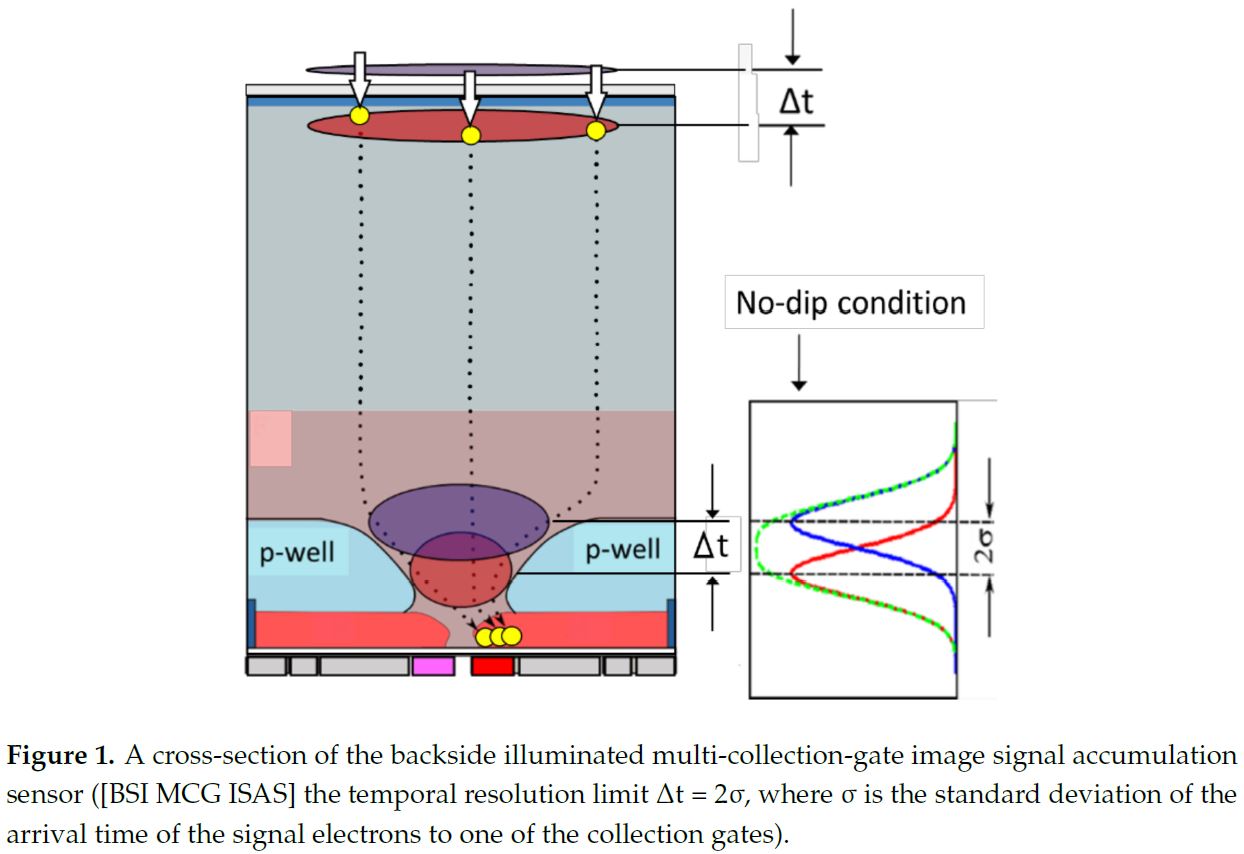
"The paper presents an ultra-high-speed image sensor for motion pictures of reproducible events emitting very weak light. The sensor is backside-illuminated. Each pixel is equipped with multiple collection gates (MCG) at the center of the front side. Each collection gate is connected to an in-pixel large memory unit, which can accumulate image signals captured by repetitive imaging. The combination of the backside illumination, image signal accumulation, and slow readout from the in-pixel signal storage after an image capturing operation offers a very high sensitivity. Pipeline signal transfer from the the multiple collection gates (MCG) to the in-pixel memory units enables the sensor to achieve a large frame count and a very high frame rate at the same time. A test sensor was fabricated with a pixel count of 32 × 32 pixels. Each pixel is equipped with four collection gates, each connected to a memory unit with 305 elements; thus, with a total frame count of 1220 (305 × 4) frames. The test camera achieved 25 Mfps, while the sensor was designed to operate at 50 Mfps."


"The paper presents an ultra-high-speed image sensor for motion pictures of reproducible events emitting very weak light. The sensor is backside-illuminated. Each pixel is equipped with multiple collection gates (MCG) at the center of the front side. Each collection gate is connected to an in-pixel large memory unit, which can accumulate image signals captured by repetitive imaging. The combination of the backside illumination, image signal accumulation, and slow readout from the in-pixel signal storage after an image capturing operation offers a very high sensitivity. Pipeline signal transfer from the the multiple collection gates (MCG) to the in-pixel memory units enables the sensor to achieve a large frame count and a very high frame rate at the same time. A test sensor was fabricated with a pixel count of 32 × 32 pixels. Each pixel is equipped with four collection gates, each connected to a memory unit with 305 elements; thus, with a total frame count of 1220 (305 × 4) frames. The test camera achieved 25 Mfps, while the sensor was designed to operate at 50 Mfps."


Comments
Post a Comment