Sony officially unveils IMX250MZR / MYR polarization sensitive image sensors. The IMX250MZR monochromatic version is available now, while color IMX250MYR is expected to be available in December 2018. The 5.07MP sensors use 3.45µm global shutter pixel with four-directional polarizer formed on the photodiode:


"With conventional types of polarization sensors, the polarizer is attached on top of the on-chip lens layer (Fig.2), however with Sony Semiconductor Solutions’ polarization sensor the polarizer is formed on chip under the on-chip lens layer (Fig.3). A shorter distance between the polarizer and the photodiode improves the extinction ratio and the incident angle dependence.
Since the polarizer is formed during the semiconductor process, form and formulation of polarizer, uniformity, mass productivity and durability are excellent compared to conventional polarization sensors. Furthermore, Sony Semiconductor Solutions’ Polarization sensor is covered with an anti-reflection layer which helps to reduce reflectance and avoids poor flare and ghost characteristics.
By creating a unique air gap structure in the polarizer, it enables excellent polarization properties and sensitivity in a broad band from visible to near infrared. It also has an advantage of excellent image quality in various light source environments by introducing the world's first anti-reflection layer to reduce flare and ghost for polarization sensor."


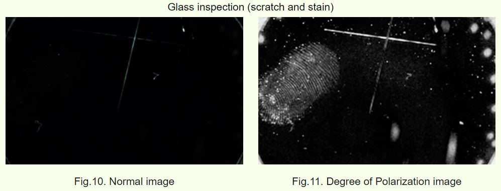
The company shows a number of examples where polarization imaging has advantages:


"With conventional types of polarization sensors, the polarizer is attached on top of the on-chip lens layer (Fig.2), however with Sony Semiconductor Solutions’ polarization sensor the polarizer is formed on chip under the on-chip lens layer (Fig.3). A shorter distance between the polarizer and the photodiode improves the extinction ratio and the incident angle dependence.
Since the polarizer is formed during the semiconductor process, form and formulation of polarizer, uniformity, mass productivity and durability are excellent compared to conventional polarization sensors. Furthermore, Sony Semiconductor Solutions’ Polarization sensor is covered with an anti-reflection layer which helps to reduce reflectance and avoids poor flare and ghost characteristics.
By creating a unique air gap structure in the polarizer, it enables excellent polarization properties and sensitivity in a broad band from visible to near infrared. It also has an advantage of excellent image quality in various light source environments by introducing the world's first anti-reflection layer to reduce flare and ghost for polarization sensor."


The company shows a number of examples where polarization imaging has advantages:


Comments
Post a Comment