A Curious Engineer Overturns Waymo Key LiDAR Patent

Ars Technica: Following a complaint by Eric Swildens, the USPTO has rejected all but three of 56 claims in Waymo's US9368936 patent. The USPTO found that some claims replicated technology described in an earlier patent from Velodyne, while another claim was simply "impossible" and "magic."

"The patent shouldn't have been filed in the first place," Swildens said. "It's a very well written patent. However, my personal belief is that the thing that they say they invented, they didn't invent."

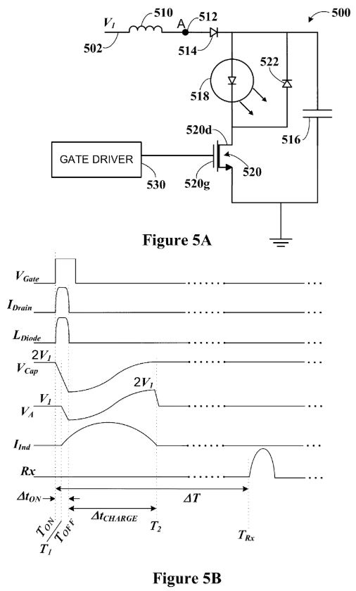
The 936 patent played a key role in last year's lawsuit with Uber. In December 2016, a Waymo engineer was inadvertently copied on an email from one of its suppliers to Uber, showing a LiDAR circuit design that looked almost identical to the one shown in the 936 patent:


Swildens said to Wired in 2017: "I couldn't imagine the circuit didn't exist prior to this patent." He then spent $6,000 of his own money to launch a formal challenge to 936 and won in the court.

Thanks to AM for the pointer!

Comments

Popular posts from this blog

Film-Based Light Sensing Review

University of Toronto repo publishes a Nature paper from January 2017 "Solution-processed semiconductors for next-generation photodetectors" by F. Pelayo GarcĂ­a de Arquer, Ardalan Armin, Paul Meredith, and Edward H. Sargent. " Efficient light detection is central to modern science and technology. Current photodetectors mainly use photodiodes based on crystalline inorganic elemental semiconductors, such as silicon, or compounds such as III–V semiconductors. Photodetectors made of solution-processed semiconductors — which include organic materials, metal-halide perovskites and quantum dots — have recently emerged as candidates for next-generation light sensing. They combine ease of processing, tailorable optoelectronic properties, facile integration with complementary metal–oxide–semiconductors, compatibility with flexible substrates and good performance. Here, we review the recent advances and the open challenges in the field of solution-processed photodetectors, examin...

Synaptics Under-Display Fingerprint Scanner Reverse Engineering

SystemPlus Consulting publishes a reverse engineering report of Synaptics’ under-display fingerprint scanner found inside the VIVO X21 UD Smartphone: " This scanner uses optical fingerprint technology that allows integration under the display. With a stainless steel support and two flexible printed circuit layers, the Synaptics fingerprint sensor’s dimensions are 6.46 mm x 9.09 mm, with an application specific integrated circuit (ASIC) driver in the flex module. This image sensor is also assembled with a glass substrate where filters are deposited. The sensor has a resolution of 30,625 pixels, with a pixel density of 777ppi. The module’s light source is providing by the OLED display glasses. The fingerprint module uses a collimator layer corresponding to the layers directly deposited on the die sensor and composed of organic, metallic and silicon layers. This only allows light rays reflected at normal incidence to the collimator filter layer to pass through and reach the optical ...

Review of Ion Implantation Technology for Image Sensors

MDPI Sensor publishes " A Review of Ion Implantation Technology for Image Sensors " by Nobukazu Teranishi, Genshu Fuse, and Michiro Sugitani from Shizuoka and Hyogo Universities and Sumitomo. " Image sensors are so sensitive to metal contamination that they can detect even one metal atom per pixel. To reduce the metal contamination, the plasma shower using RF (radio frequency) plasma generation is a representative example. The electrostatic angular energy filter after the mass analyzing magnet is a highly effective method to remove energetic metal contamination. The protection layer on the silicon is needed to protect the silicon wafer against the physisorbed metals. The thickness of the protection layer should be determined by considering the knock-on depth. The damage by ion implantation also causes blemishes. It becomes larger in the following conditions if the other conditions are the same; a. higher energy; b. larger dose; c. smaller beam size (higher beam current d...