Taiwan-based Artilux' paper "Proposal and demonstration of lock-in pixels for indirect time-of-flight measurements based on germanium-on-silicon technology" by N. Na, S.-L. Cheng, H.-D. Liu, M.-J. Yang, C.-Y. Chen, H.-W. Chen, Y.-T. Chou, C.-T. Lin, W.-H. Liu, C.-F. Liang, C.-L. Chen, S.-W. Chu, B.-J. Chen, Y.-F. Lyu, and S.-L. Chen unveils the company plans to work with TSMC on Ge-on-Si pixel:
"We propose the use of germanium-on-silicon technology for indirect time-of-flight depth sensing as well as three-dimensional imaging applications, and demonstrate a novel pixel featuring a high quantum efficiency and a large frequency bandwidth. Compared to conventional silicon pixels, our germanium-on-silicon pixels simultaneously maintain a high quantum efficiency and a high demodulation contrast deep into GHz frequency regime, which enable consistently superior depth accuracy in both indoor and outdoor scenarios. Device simulation, system performance comparison, and electrical/optical characterization of the fabricated pixels are presented. Our work paves a new path to high-performance time-of-flight sensors and imagers, as well as potential adoptions of eye-safe lasers (wavelengths > 1.4um) that fall outside of the operation window of conventional silicon pixels."
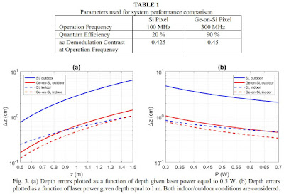
"These results might be surprising as the dark current of the Ge-on-Si pixel is set to be several orders of magnitude larger than that of the Si pixel (nearly no changes to Fig. 3(a) and 3(b) even if a lower Si pixel dark current is set). The reason lies in that, in an indirect TOF system, the dominant system noise is in fact due to the indoor/outdoor ambient light and the laser light instead of the dark current for various depth sensing and 3D imaging applications."
The company patent applications, such as US20170040362, show the proposed pixel structures:


Comments
Post a Comment